My First PCB has Just Arrived
Having been working on FPGA for a while, and I realized that sooner or later I’ll have to deal with designing my own PCB: whether it’s a small extension board of functions that commercially available PMOD connectors and modules can’t satisfy, or my own low cost FPGA development board with chips scavenged from second hand markets. The first is what this article is about, and the second is… well, on my TODO list but may take years to begin, let alone finish.
Time flies, the PCB arrived at the beginning of October, 2020, the above paragraph was written more than two month ago, and now it’s about Christmas and a lot has changed. I didn’t have time to debug my first small 5-yuan PCBs until last month, and now I can finally finish this blog article.
And about the second project(self-designed FPGA board), it’s going surprisingly well – I managed to finish schematic and layout which were literally my only “extracurricular activity” during the busy application season. And now I’m soldering and debugging the boards, which do seem to have problems but in general are pretty fine. I’m confident to finish it before graduation, and may even sell one or two to cover the cost(I’ve spent more than a Cyberpunk 2077 on this project so far).
So get back to the main point now.
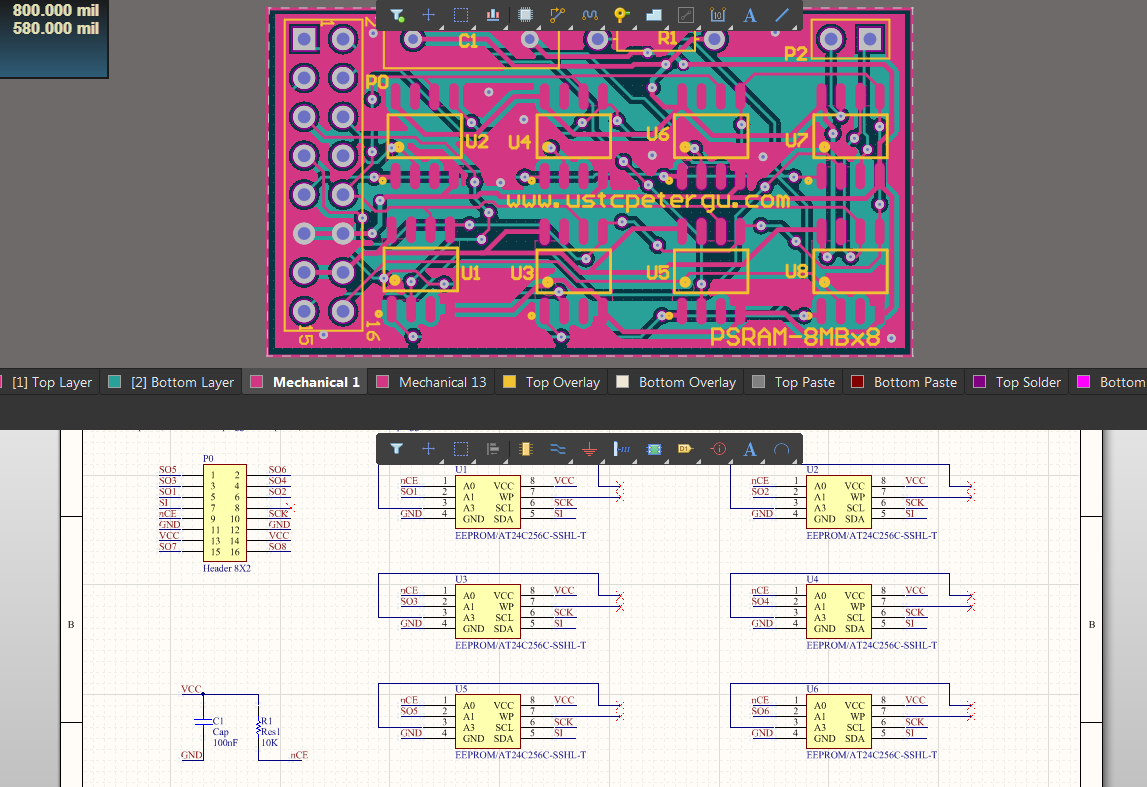
Background: I need main memory for my FPGA-based homebrewed simple computer. I don’t have DDR on PL side on my xc7z020 @ PYNQ-Z1. Don’t want to trouble myself with AXI. A small extension board with some PSRAM(Pseudo Static RAM, the thing used on the old Digilent Nexys4) would be fine: I’m using ESP-PSRAM64H, cheap, 8MByte, SPI interface is enough, easy soldering.
I had zero PCB design knowlege 3 month earlier, and learning EDA software (for now I use Altium Designer in VMWare, but I really want to migrate to KiCAD later) was easier than thought: after some videos and a tutorial book, I grabbed the basic procedure: find footprint and models for your components, draw the schematic, know the processing limit of where you want to have the board made, do the layout using the extremely convenient software, run a check, and done. It was a little annoying to get the model and footprint you want at first, so I have to use a combination of the default Altium libs, libs from JLCPCB, as well as some libs from GitHub. The schematic was relatively simple. I didn’t have any layout experience but hey, some small SOP8 chips won’t be so hard! I do placed 13 vias on one line but, it’s my first time! Then it was submitted to manufacture companies with the cheapest options, which was, again, a seemingly frightening but actually easy step.
Here’s the design:
And right before it’s arrival I found problems: I though it were like SRAM-style memories that share the same address line and only data inputs and outputs are combined, so I drew a same input for all chips. But it’s SPI! input of address and data are using the same line! Oh, time to fly wires. Black PCB hurt eyes.
Here’s the final version:

Then plug it into my PYNQ-Z1 and start debugging with datasheet, ILA, and multimeter. Three day passed and I found it’s the power on condition that kept the chip silent. Should use “inout” variable type and keep both MISO and MOSI low during power on. I was near the FPGA hell.
But anyway, that’s a low of fun.
 This work is licensed under the Creative Commons BY-SA 4.0 International License, if not explicitly specified.